Table Of Content

All the PCB software we’ve reviewed generally offer the same core layout and schematic design features, but the quality varies a lot depending on the program. For example, the 3D renderings offered by professional solutions like Altium are considerably higher quality than those you get in free programs. Plus, as it’s technically part of Fusion 360, you have seamless integration with a vast array of advanced CAD, CAM, and CAE tools, making it a great all-in-one solution for many electrical engineering applications. In a nod to accessibility, EasyEDA dodges the need for a beefy PC to create and render PCB designs with a browser-based option that works whether you’re on Windows, Mac, Linux, or even a smartphone.
Recyclable vitrimer-based printed circuit boards for sustainable electronics
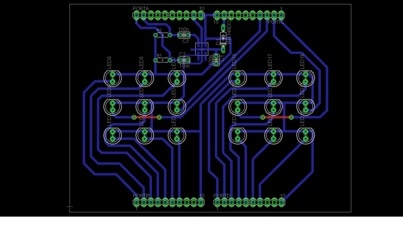
Before routing your traces, it is a good idea to place your drill holes (mounting and vias). If your circuit board design is complicated you may need to modify at least some of the via locations during trace routing. It's also important to annotate your schematics, as well as name nets when schematics get large and complex. As higher pin count devices are added to schematics, you can use net name assignments to keep things organized and easily track connectivity between components.
DIP (Dual in-line packages)
For example, it’s not uncommon to see offers of 5 copies of your board for less than $5 USD! When you’re done drawing the board, you can either send the design to a manufacturer that will make it for you (it’s actually pretty cheap) – or you can etch it yourself at home. See our Engineering Essentials page for a full list of cornerstone topics surrounding electrical engineering.
Multiplexer (MUX) and Demultiplexer (DEMUX) Applications
The material is tactilely reminiscent of a film roll, and the board thickness is usually far less than a standard rigid board. While they already see major usage, there is hope that flexible boards will usher in the next step of wearable technology and remove the current planar constraints inherent to rigid board devices. The package is what encapsulates the integrated circuit die and splays it out into a device we can more easily connect to.
This layer helps the user to solder to the correct places and prevent solder jumpers. The copper thickness can vary and is specified by weight, in ounces per square foot. The vast majority of PCBs have 1 ounce of copper per square foot but some PCBs that handle very high power may use 2 or 3 ounce copper.
Unique Features and Services of EasyEDA
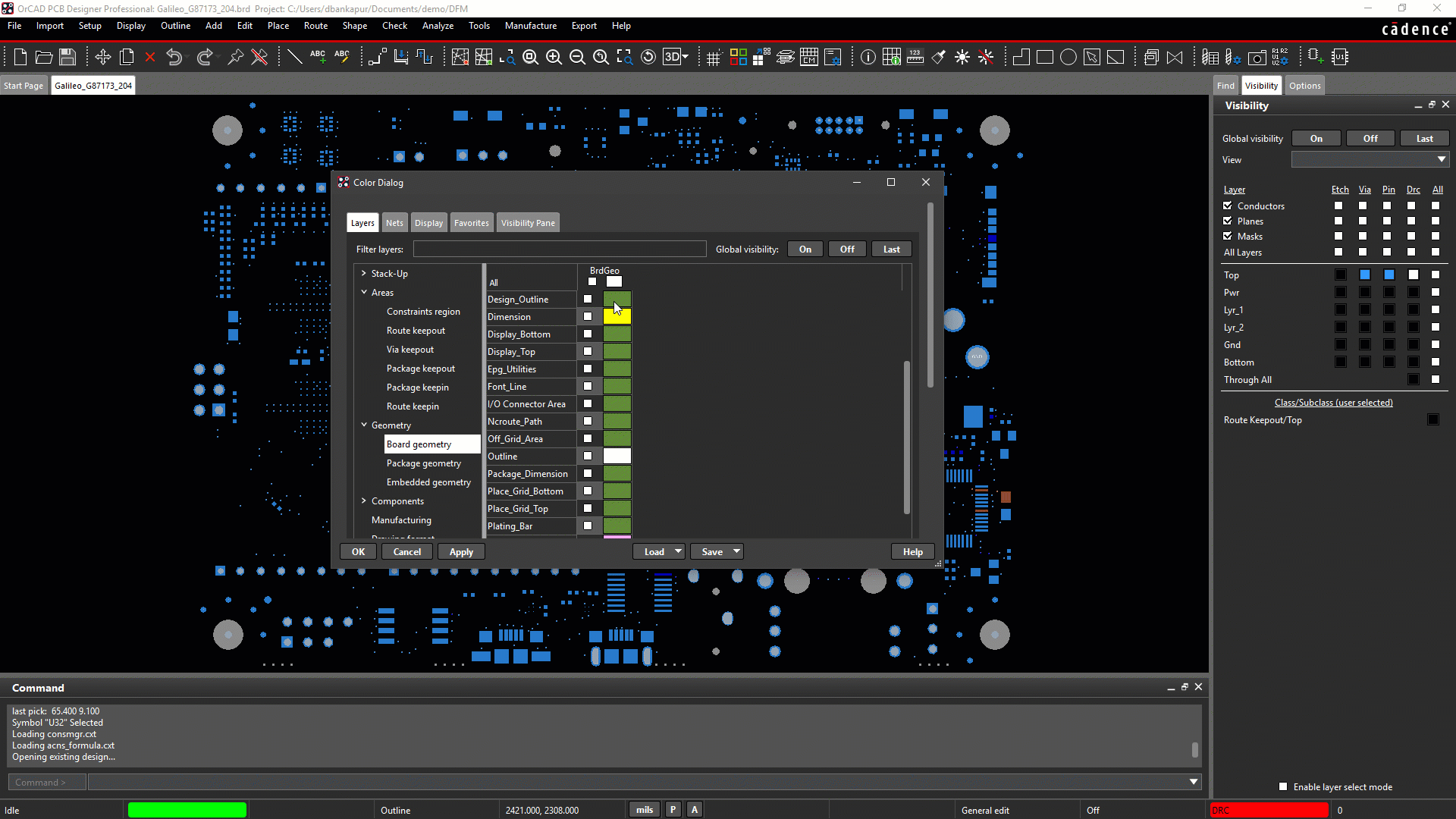
In order to work with surface-mount packaged ICs, you usually need a custom printed circuit board (PCB) made for them, which has a matching pattern of copper on which they're soldered. Your preferences here should be guided by the design for manufacturing (DFM) specifications of your PCB manufacturer. If you already defined your PCB DFM requirements as design rules (see Step 5), Altium Designer will automatically check these rules as you place vias, drill holes, pads, and traces in your layout.
All PCBs are built from alternating layers of conductive copper with layers of electrically insulating material. Conductive features on printed circuit boards include copper traces, pads, and conductive planes. The mechanical structure is made up of the insulating material laminated between the layers of conductors. The overall structure is plated and covered with a non-conductive solder mask, and silk screen is printed on top of the solder mask to provide a legend for electronic components.
Thermal design optimization of electronic circuit board layout with transient heating chips by using Bayesian ... - ScienceDirect.com
Thermal design optimization of electronic circuit board layout with transient heating chips by using Bayesian ....
Posted: Sun, 28 Nov 2021 14:00:41 GMT [source]
Copper
We use red for almost all the SparkFun boards, white for the IOIO board, and purple for the LilyPad boards. In the example below, the green solder mask is applied to the majority of the PCB, covering up the small traces but leaving the silver rings and SMD pads exposed so they can be soldered to.
Step 6: Place Components
Italy sets up chips design centre in Pavia, attracts industry leaders - Decode39 English
Italy sets up chips design centre in Pavia, attracts industry leaders.
Posted: Tue, 07 Nov 2023 08:00:00 GMT [source]
There’s no denying that some software are better designed and easier to use than others, and it’s often the more professional paid solutions that are the most intuitive. For example, if you compare an open-source program like Fritzing PCB design software to a professional program like Altium, the latter is noticeably better laid out, has a sleeker design, and is much more intuitive. Another benefit of OrCAD is the dynamic differential pair routing, which makes it easy to meet length and phase pin-to-pin constraints because traces can bend without causing any electrical issues. You can switch between 2D and 3D in this software’s highly intuitive and interactive environment, allowing you to examine each aspect of your layouts.
It's impossible to manually connect all of these components together with soldered wires, so the copper connections are deposited directly on insulating substrates as described in the above manufacturing process. Many of today's devices are advanced high density interconnect (HDI) designs with thousands of connections and multiple electrical interfaces, powering everything from smartphones to heart rate monitors to rockets. Usually, each active component on the board (ICs and other related components) need to be connected to power and ground nets. This is easily accomplished by flooding areas or layers with solid planes that these components can tap into. These planes also do the important job of returning the signals that are routed with traces. If the planes have too many holes, cut-outs, or splits, it can cause these return paths to create a lot of noise and degrade the performance of the PCB.
This original substrate was initially a material called bakelite, which was used to replace the top ply on a sheet of plywood. The number of wires was so great that they could get tangled or inhabit a large space within a design. Manufacturing was also slow, where multiple components and their wired connections were manually soldered. PCB designers follow a general PCB design process methodology, and there are some important things to consider in your schematic and layout before you get started.
The SSOP (shrink small-outline package) is an even smaller version of SOIC packages. Other, similar IC packages include TSOP (thin small-outline package) and TSSOP (thin-shrink small-outline package). Here are a few of the more common SMD package types out there, ranging in hand-solderability from "doable" to "doable, but only with special tools" to "doable only with very special, usually automated tools". When you’re finished drawing your PCB design, you need to get the design made. You could etch your PCB at home, but my preferred way is to just order a PCB from one of the many PCB manufacturers out there.
Altium Designer displays attributes for all layers in a color-coded workspace. You’ll have the best PCB design technology on the market when you use Altium Designer. PCB designers used to be forced into using multiple programs with a rigid workflow to create a schematic and PCB layout. Now, innovations in PCB design software allow PCB designers to create a PCB design process methodology around complex key features in their circuit board layout.


No comments:
Post a Comment